Back to: AND gate
What is an AND gate?
An AND gate has two inputs and one output. It is called an AND gate because its output level is 1 when one of its INPUTS is 1 AND the its other INPUT is 1. For all other combinations its OUTPUT is 0.
How can we construct an AND gate?
There are numerous ways but the way that I want to show you is using 2 switches, 3 resistors and 2 transistors.
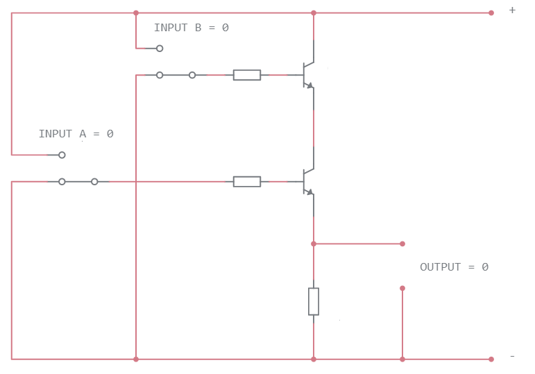
Figure 1.1 is an AND gate that has both of its inputs connected to a negative voltage. Both of the transistors are switched off and there is no path through the collectors and emitters, acting like an open circuit (this is known as cut off). This results in the output being off.
We can say that when INPUT A is OFF AND INPUT B is OFF, the OUTPUT is OFF.
Or when INPUT A is 0 AND INPUT B is 0, the OUTPUT is 0.
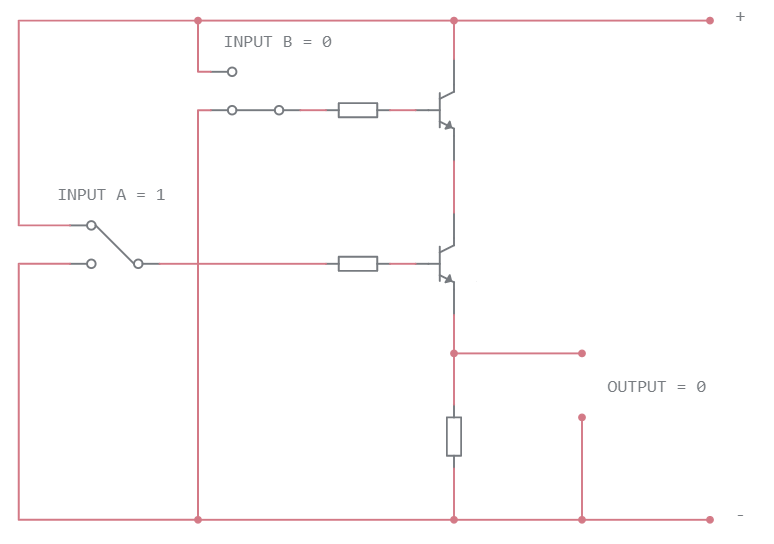
In figure 1.2 and figure 1.3 there is an AND gate that has one of its inputs connected to a negative voltage and the other to a positive voltage. One of the transistors is switched off and there is no path through its collector and emitter, acting like an open circuit (this is know as cut off). The other transistor is switched on and there is a path through its collector and emitter, so that it acts like a closed circuit (this is known as satuation). However, because the collectors and emitters are in series with each other, there is no complete circuit. This results in the output being off.
For figure 1.2 we can say that when INPUT A is ON AND INPUT B is OFF, the OUTPUT is OFF.
Or when INPUT A is 1 AND INPUT B is 0, the OUTPUT is 0.
For figure 1.3 we can say that when INPUT A is OFF AND INPUT B is ON, the OUTPUT is OFF.
Or when INPUT A is 0 AND INPUT B is 1, the OUTPUT is 0.
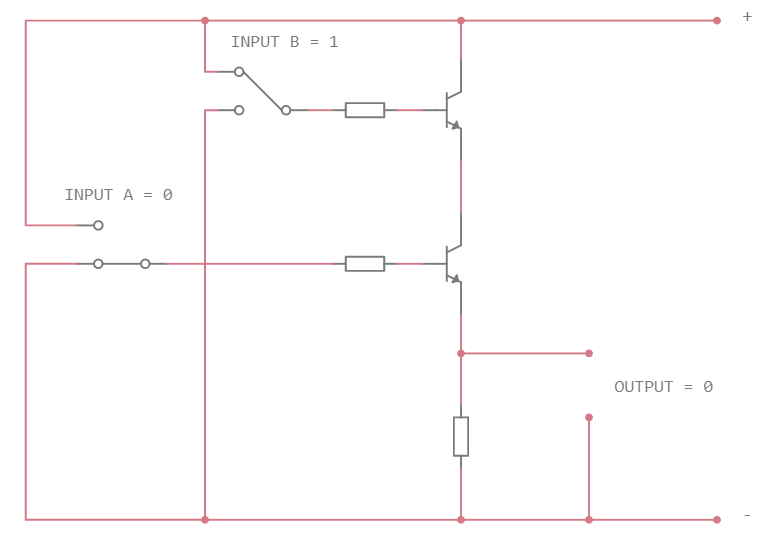
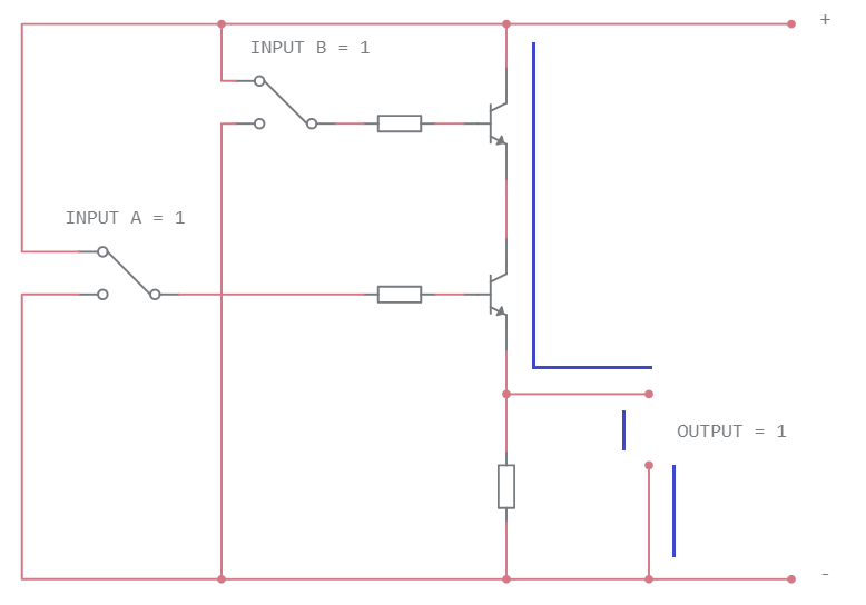
Figure 1.4 is an AND gate that has both of its inputs connected to a positive voltage. Both of the transistors are switched on and there is a path through both of the collectors and emitters, acting like a closed circuit (this is known as saturation). There is a complete circuit and the output is on.
We can say that when INPUT A is ON AND INPUT B is ON, the OUTPUT is ON.
Or when INPUT A is 1 AND INPUT B is 1, the OUTPUT is 1.
Using Boolean algebra we can say that OUTPUT = A.B
Truth table for an AND gate
[table “” not found /]
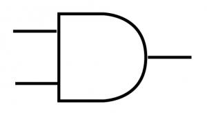
Symbol for an AND gate
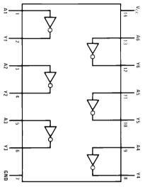
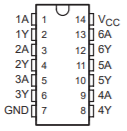
7408 quad AND gate
There are a number of ICs that contain AND gates. In the 74 series one of these is the 7408. This is a 14 pin IC, containing 4 AND gates.
Figure 1.3 shows the pinout of a 7408. The negative voltage needs to be applied to pin 7 and the positive voltage to pin 14.
If you look at figure 1.4 you can see how the AND gates are arranged.